The question to be answered is simple. If there are direct and indirect semiconductors where electroncs trasition from valence band to conduction band, are there mateirals that can leverage advantange of both the types of materials? In this con- text, two-dimensional (2D) materials with few atomic layers thickness have shown particular promise for photodetector applications owing to their large surface area, pristine surfaces, tunable electronic properties, and mechanical flexibility. The broadband photodetectors convert the incident electromagnetic radiations over a wide range of wavelengths into electrical signals for detection. The detection mechanism is governed by the interactions of electromagnetic radiation with photoabsorbing material and, subsequently, the choice of such material principally determines the performance of photodetectors
A wide range of 2D materials is realized and eventually exploited for ultrafast and ultra- sensitive detection of lights in terahertz, infrared, visible, and ultraviolet frequency ranges. In this line, transition metal dichalcogenide (TMD) has emerged as one of the potential 2D semiconductors for optoelectronic applications owing to the presence of suitable energy bandgaps (1–2 eV) that can be tuned by changing the layer thick- ness. Moreover, TMDs exhibit transition from an indirect to direct bandgap between their multilayers and monolayer configurations.
The weak van der Waals (vdW) interaction between individual layers of 2D mate- rials allows the realization of designer heterostructure materials by vertically stack- ing one or a few layers of two dissimilar 2D materials. These structures are usually referred to as vdW hetero structures having atomically sharp interfaces where emer- gent properties can be observed
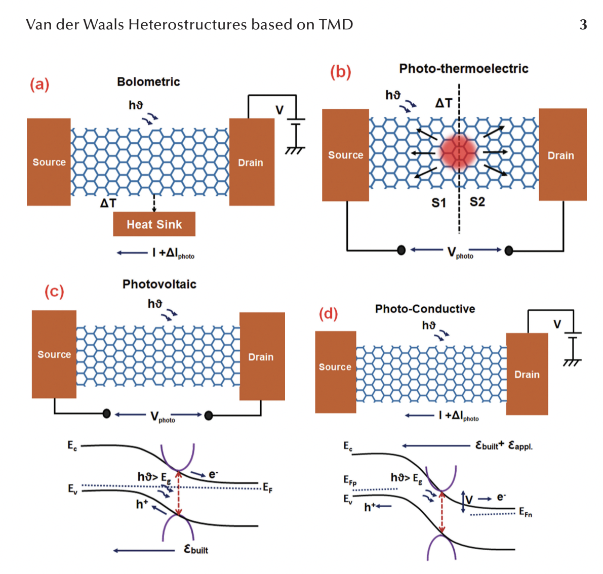

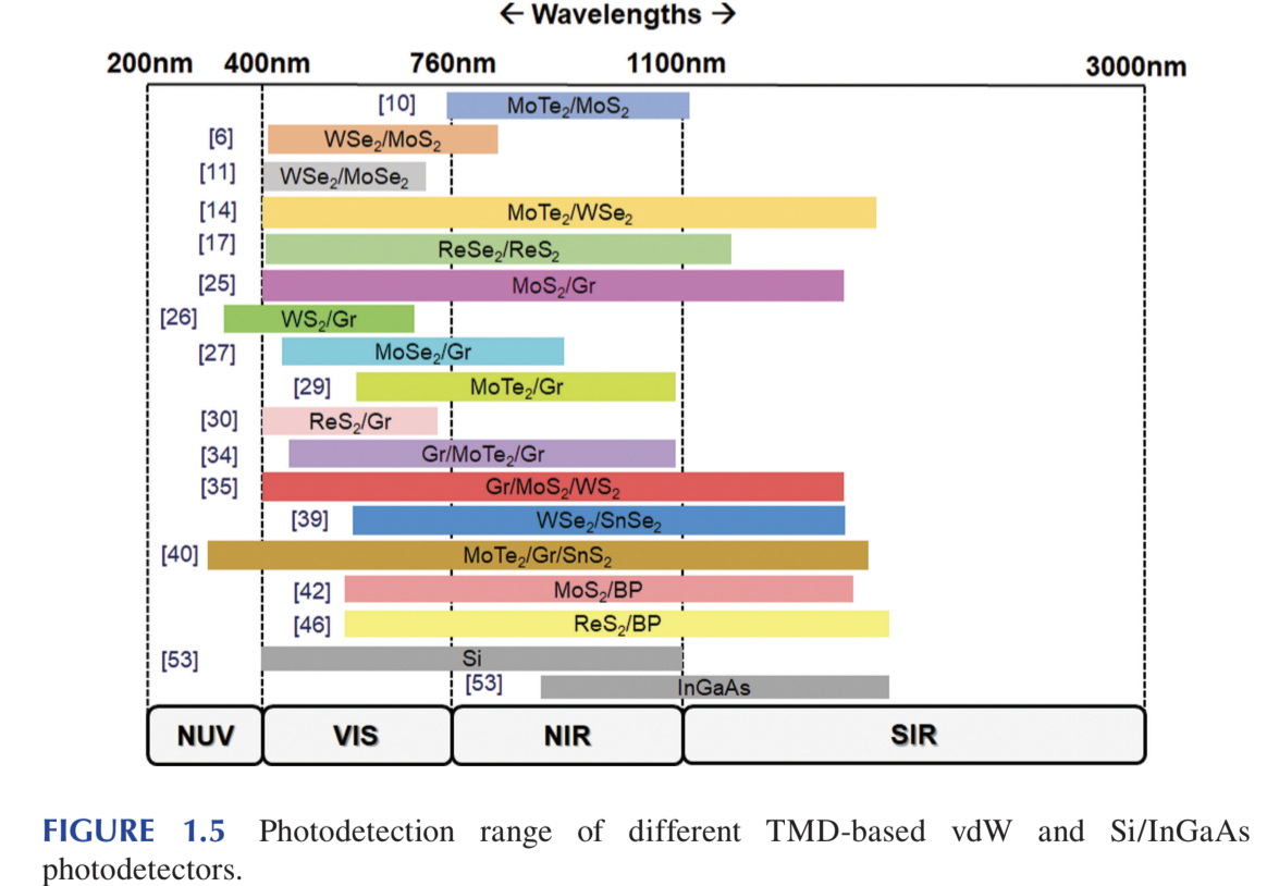
The study indicates that, in general, the TMD-based vdW photodetectors exhibit comparable or superior responsivity, EQE, as well as a detectable wavelength range than that of Si- and InGaAs-based photodetectors. This can be attributed to the interlayer photocarrier generation as well as special charge-separation at the vdW heterointerfaces which is most effectively tuned by stacking different 2D semiconductors or semimetal (Gr) with TMDs. A superior photoresponse in both photovoltaic (without applied bias) and photoconductive (under applied bias) modes can be observed. At the same time, the light-matter interaction at the vdW interface exhibits a unique feature, where absorption of incident radiations corresponding to a bandgap lesser than that of constituent TMDs can be observed.
TMD-based vdW broadband photodetectors are typically suitable for highly sensitive photodetection applications without ultrahigh speed requirement.
Published on - Van der Waals (VdW) Hetero structures based on Transition Metal Di-Chalcogenides (TMD) -Current Status and Prospects in Broad-Band Photo-detector Applications, Debapriya Som, Srijan Trivedi, Ayantika Chatterjee, Sayan Kanungo, Microelectronics and Signal Processing: Advanced Concepts and Applications, Taylor & Francis (ISBN 9780367640125)